AKD SynqNet I/O Mapping
The following tables show the mapping from AKD physical pin names to SynqNet logical names.
These tables show mapping for FPGAs, version 0200_00_02 and later.
General Purpose I/O
| AKD Firmware | AKD Connector | AKD Pin Name | SynqNet MPI Name | Notes |
|---|---|---|---|---|
| DIN1.STATE | X7-10 | Digital Input 1 | GPIO input "DIN 1 (HS)" | High speed opto input. Also maps to HOME. |
| DIN2.STATE | X7-9 | Digital Input 2 | GPIO input "DIN 2 (HS)" | High speed opto input. |
| DIN3.STATE | X7-4 | Digital Input 3 | GPIO input "DIN 3" | |
| DIN4.STATE | X7-3 | Digital Input 4 | GPIO input "DIN 4" | |
| DIN5.STATE | X8-6 | Digital Input 5 | GPIO input "DIN 5" | Also maps to "LIMIT_HW_POS". |
| DIN6.STATE | X8-5 | Digital Input 6 | GPIO input "DIN 6" |
Also maps to "LIMIT_HW_NEG". |
| DIN7.STATE | X7-2 | Digital Input 7 | GPIO input "DIN 7" | |
| DIN9.STATE DIO9.STATE |
X9-1/2 | Emulated Encoder A | GPIO bidir "RS485 IO 1" | See note to enable output. |
| DIN10.STATE DIO10.STATE |
X9-4/5 | Emulated Encoder A | GPIO bidir "RS485 IO 2" | See note to enable output. |
| DIN11.STATE DIO11.STATE |
X7-7/8 | Emulated Encoder Zero | GPIO bidir "RS485 IO 3" | See note to enable output. Also maps to "INDEX_SECONDARY." |
| DOUT1.STATE | X7-8/7 | Digital Output 1 | GPIO output "DOUT1" | |
| DOUT2.STATE | X7-6/5 | Digital Output 2 | GPIO output "DOUT1" | |
| NA | X10-6/7 | Zero | GPIO input "Analog Z Pulse" | Also maps to "INDEX_PRIMARY." Some encoder types do not use index pin. |
Notes:
- The RS485 outputs must be enabled using AKD-SQ parameters.
- Set DRV.EMUMODE = 10 (fieldbus) for SynqNet gpio output mode.
- Set DIO9.DIR=1, DIO10.DIR=1, DIO11.DIR=1 to enable individual outputs.
- GPIO input "Analog Z Pulse" not supported on AKD Rev 7 control boards (AKD-SQ prototypes only).
Dedicated I/O
| AKD Firmware | AKD Connector | AKD Pin Name | SynqNet MPI Name | Notes |
|---|---|---|---|---|
| DIN1.STATE | X7-10 | Digital Input 1 | Dedicated input "HOME" | High speed opto input. Also maps to DIN 1 (HS). |
| DIN5.STATE | X8-6 | Digital Input 5 | Dedicated input "LIMIT_HW_POS" | Also maps to "DIN 5." |
| DIN6.STATE | X8-5 | Digital Input 6 | Dedicated input "LIMIT_HW_NEG" | Also maps to "DIN 6." |
| DIN11.STATE | X9-7/8 | Emulated Encoder Zero | Dedicated input "INDEX_SECONDARY" | Also maps to "RS485 IO 3." |
| NA | X10-6/7 | Zero | Dedicated input "INDEX_PRIMARY" | Also maps to "Analog Z Pulse." Some encoder types do not use index pin. |
| NA | X8-1/2 | Fault Relay Output | Dedicated input "AMP_FAULT" | Logical OR of AKD and SynqNet faults |
| FB1.HALLSTATEU | X10-1 | Hall U | Dedicated input "Hall A" | See note on bit order |
| FB1.HALLSTATEV | X10-2 | Hall V | Dedicated input "Hall B" | See note on bit order |
| FB1.HALLSTATEW | X10-3 | Hall W | Dedicated input "Hall C" | See note on bit order |
| MOTOR.BRAKESTATE | Dedicated output "BRAKE_RELEASE"
Dedicated input "BRAKE_APPLIED" |
Brake release is command from SynqNet Brake applied is status from AKD drive (logical OR) |
Notes:
- Hall input bit order is swapped in beta release FPGAs. Planned (corrected) order shown above.
- For AKD FPGA versions 0200 and prior, AKD U/V/W maps to Hall C/B/A.
- For AKD FPGA versions TBD and later, AKD U/V/W maps to Hall A/B/C.
- GPIO input "Analog Z Pulse" not supported on AKD Rev 7 control boards (AKD-SQ prototypes only).
Node I/O
| AKD Firmware | AKD Connector | AKD Pin Name | SynqNet MPI Name |
|---|---|---|---|
| AOUT.VALUE | X8-7/8 | Analog Output | Nodelo AnalogOut[0] output |
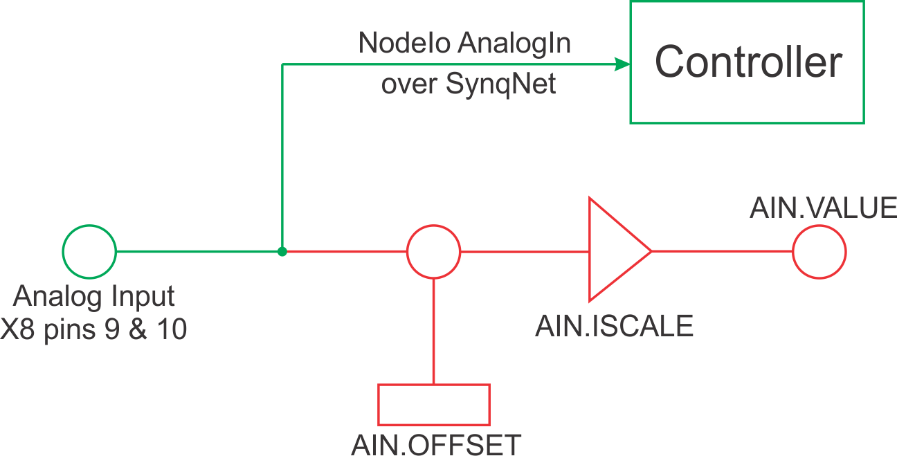
| AIN.VALUE | X8-10/9 | Analog Input | Nodelo AnalogIn[0] input |
Analog Output
When the AKD SynqNet drive enters normal cyclic operation, AOUT.MODE is automatically set to 12 (SynqNet AnalogOut), and the SynqNet controller sends the NodeIo AnalogOut value directly to the AKD's Analog Output pins. AOUT.MODE does not allow other values, and the filter and scaling is bypassed. AOUT.VALUE does not read back the AnalogOutput value. AOUT.VALUEU is ignored.
AOUT.MODE = 12:

Analog Input
When the AKD SynqNet drive enters normal cyclic operation, AIN.MODE is automatically set to 0 (Monitor), and the drive sends the raw AnalogInput value to the SynqNet controller as NodeIo AnalogIn. The offset and scale are bypassed.


